Products
Graphene on Si | SiO2
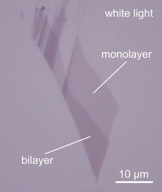
The most common substrate for graphene is oxidised silicon. Monolayer graphene is readily visible in white light if the thickness of silicon dioxide is carefully chosen to maximise the contrast. We offer single, double, triple and >3 layer graphene flakes on 300 nm and 90 nm SiO2. 90 nm SiO2 is a new substrate that offers higher graphene contrast than the traditional 300 nm (for more information, read Making graphene visible by Blake et al.).
You can view our current stock of graphene samples in our Sample Catalog. If there are no samples that meet your specification, please contact us and we will do our best to satisfy your requirements. We prepare new graphene flakes every week to meet orders; samples are often sold before they have a chance to appear in the catalog.
| Flake sizes | Largest monolayer found to date: 1,500,000 μm2, but typically < 2000 μm2 |
|---|---|
| Pricing guide | ≈ £ 0.50 per μm2 area (decreases significantly for v. large flakes), with reductions if the flake is difficult to use for lithography, e.g. close to wafer's edge or surrounded by thick graphite flakes |
| Applications | transistors, spintronics, gas sensors, metrology, Raman spectroscopy, AFM, STM, etc. |
| Wafer sizes | min: 5 mm × 5 mm; max: 76 mm diameter circle |
Graphene on electrically conductive substrate
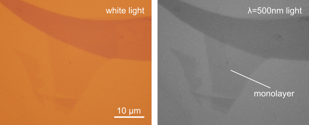
We can isolate graphene flakes on gold using optical microscopy. A thin layer of gold is deposited onto an oxidised silicon wafer before preparing flakes. The gold layer is continuous and electrically conductive, but thin enough to maintain the optical interference effect that makes graphene visible. Narrow band-pass filters can be used to enhance the contrast (image comparison below).
The graphene flakes are in electrical contact with the substrate - useful for certain applications, such as STM.
| Flake sizes | Largest monolayer found to date: 5000 μm2, but typically < 500 μm2 |
|---|---|
| Pricing guide | ≈ £ 3 per μm2 area |
| Applications | STM, Raman spectroscopy |
| Wafer sizes | min: 5 mm × 5 mm; max: 25 mm × 25 mm |